
Artificial Intelligence is no longer confined to software and cloud data centres. It has firmly entered the hardware domain — transforming how printed circuit boards are designed, manufactured, tested, and powered. From AI chips like NVIDIA's H100 and Google's TPU that demand unprecedented power delivery, to machine learning algorithms that optimize PCB layout and detect manufacturing defects invisible to the human eye — the AI-PCB convergence is reshaping the electronics industry.
In this article, the AEAR team explores the multi-dimensional relationship between AI and PCB technology — examining both how PCBs enable AI hardware and how AI is revolutionizing PCB engineering itself.
Market Snapshot
The global AI chip market is projected to exceed $230 billion by 2033, growing at a CAGR of over 29%. Every AI accelerator — whether in a data centre, an autonomous vehicle, or an edge device — requires highly sophisticated power supply PCBs to function reliably.
1. Introduction: The AI-PCB Convergence
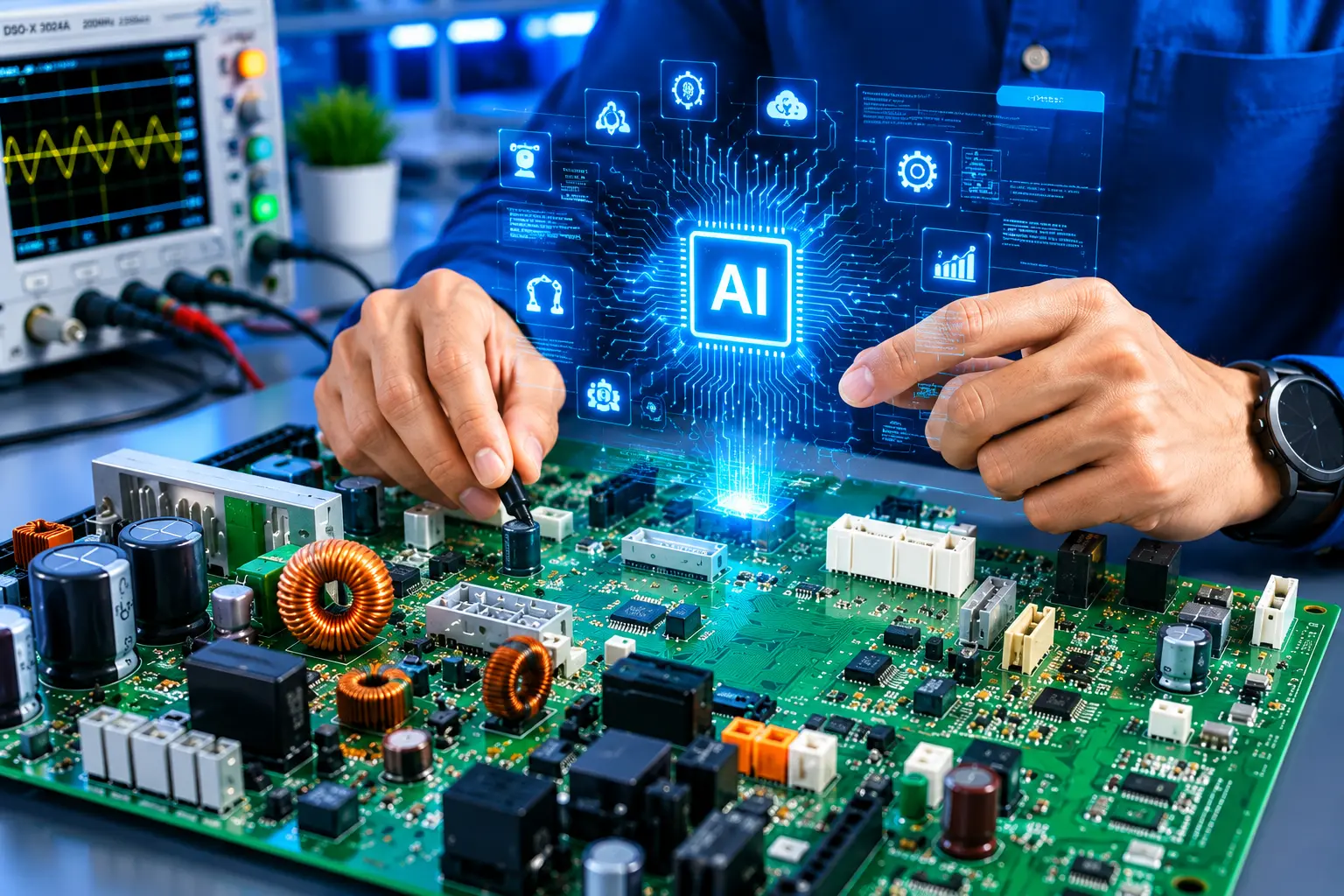
The relationship between artificial intelligence and printed circuit boards is bidirectional. On one hand, AI processors — GPUs, TPUs, NPUs, and FPGAs — are among the most power-hungry and thermally challenging components ever placed on a PCB, demanding breakthroughs in power delivery, thermal management, and signal integrity. On the other hand, AI and machine learning tools are increasingly being used to design better PCBs, detect defects during manufacturing, and optimize the entire electronics production workflow.
Understanding this convergence is essential for any engineer, manufacturer, or technology leader navigating the rapidly evolving electronics landscape.
2. AI-Optimized Power Efficiency
AI processors are notorious for their power consumption. An NVIDIA H100 GPU can draw 700 watts, and a fully populated AI server rack can consume over 40 kW. Delivering this power efficiently — with minimal losses — is one of the greatest challenges in modern PCB design.
AI-optimized power supply PCBs employ several advanced techniques: multi-phase voltage regulators that share current across 8, 12, or even 16 parallel phases to handle hundreds of amperes at sub-1V core voltages; gallium nitride (GaN) and silicon carbide (SiC) power semiconductors that switch at MHz frequencies with dramatically lower losses than traditional silicon MOSFETs; and digital power management with PMBus/I²C telemetry that allows AI systems to dynamically adjust voltage levels based on workload — reducing power consumption during idle or light-load periods by 30-50%.
3. Robust Power Distribution Networks for AI Hardware
A modern AI accelerator PCB may have over 20 power rails, each requiring precise voltage regulation with tolerances as tight as ±1%. The Power Distribution Network (PDN) — the system of voltage regulators, decoupling capacitors, power planes, and vias that delivers clean power to every component — must be designed with extraordinary care.
Key PDN design principles for AI PCBs include: target impedance analysis to ensure the PDN impedance remains below the maximum allowed across the entire frequency spectrum (DC to GHz); strategic placement of decoupling capacitors with different values (e.g., 100 nF, 10 nF, 100 pF) to cover different frequency ranges; embedded capacitance using thin laminate layers (< 50 µm) between power and ground planes for distributed high-frequency decoupling; and power plane stitching with dense via arrays to minimize inductance between layers.
4. Compact Form Factors & Miniaturization
AI is increasingly moving to the edge — from data centres into smartphones, drones, autonomous vehicles, and IoT devices. This demands PCBs that pack massive computational capability into incredibly small form factors. Techniques driving this miniaturization include: HDI (High-Density Interconnect) with laser-drilled microvias (as small as 50 µm), any-layer via technology that allows connections between any adjacent layers, component embedding where passive components and even some ICs are buried inside the PCB substrate, and rigid-flex designs that fold three-dimensional circuitry into tight enclosures.
Power supply sections for edge AI devices face additional constraints: they must deliver high peak currents for AI inference bursts while maintaining ultra-low quiescent current during sleep modes — often below 1 µA — to preserve battery life in always-on applications like voice assistants and wearable health monitors.
5. AI-Driven Signal Integrity & Noise Reduction
The high-speed digital interfaces connecting AI processors to memory (HBM3/HBM4 with 1024-bit wide buses at 6-8 Gbps per pin), storage (PCIe Gen5/6 at 32-64 GT/s), and networking (200G/400G Ethernet, NVLink, Infinity Fabric) push signal integrity to its absolute limits. At these data rates, every via stub, impedance discontinuity, and crosstalk aggressor matters.
AI-powered EDA (Electronic Design Automation) tools are now capable of automated signal integrity optimization — using genetic algorithms and reinforcement learning to explore thousands of routing topologies and identify the one with optimal eye diagram opening, minimal jitter, and lowest crosstalk. These tools can also perform power-aware SI analysis, accounting for simultaneous switching noise (SSN) from hundreds of I/O buffers switching in unison — a critical effect in AI accelerator PCBs.
6. Machine Learning for PCB Inspection & Testing
One of the most impactful applications of AI in PCB manufacturing is automated optical inspection (AOI) and automated X-ray inspection (AXI) powered by deep learning. Traditional AOI systems use rule-based algorithms that compare captured images to a golden board — effective for obvious defects but prone to false positives and missed subtle anomalies.
Deep learning-based inspection systems, trained on millions of labelled PCB images, can detect solder joint defects (insufficient solder, bridging, head-in-pillow, voids), component placement errors (tombstoning, skew, wrong orientation), trace defects (opens, shorts, neckdowns, nicks), and even counterfeit component indicators with accuracy exceeding 99.5%. These systems continuously improve as they're exposed to more data, reducing both false-positive rates and the need for manual review.
AEAR AI Inspection
At AEAR, we employ AI-enhanced AOI and X-ray inspection systems that achieve sub-10-micron defect detection across 100% of production. Combined with our expert human inspectors, this dual-layer quality assurance ensures Class 3 reliability for mission-critical PCBs.
7. AI-Assisted PCB Design Automation
PCB design has historically been a manual, expertise-intensive process — component placement, routing, and verification can take weeks or months for complex boards. AI is changing this paradigm through: auto-routing engines that use deep reinforcement learning to produce routings competitive with experienced human designers; placement optimization that minimizes total wire length, crosstalk, and thermal hotspots simultaneously; design rule checking (DRC) enhanced with ML that predicts manufacturability issues before fabrication; and generative design where AI proposes multiple PCB layouts meeting given constraints, allowing engineers to select and refine the best option.
While AI is not yet replacing PCB designers, it is dramatically amplifying their productivity — handling the tedious, iterative aspects of routing and verification so engineers can focus on architecture, component selection, and system-level trade-offs.
8. Energy Harvesting & Sustainable AI Hardware
The environmental impact of AI computing is becoming a critical concern. Training a single large language model can consume gigawatt-hours of electricity. At the hardware level, energy harvesting techniques integrated into PCBs offer a path toward more sustainable AI: thermoelectric generators (TEGs) that convert waste heat from AI chips back into usable electricity; piezoelectric energy harvesters that capture vibration energy in industrial and automotive environments; photovoltaic cells integrated onto PCBs for solar-powered edge AI sensor nodes; and RF energy harvesting that captures ambient wireless signals to power ultra-low-power AI inference chips.
While these technologies currently harvest milliwatts rather than watts, they are enabling a new class of batteryless, maintenance-free AI sensor nodes for applications in structural health monitoring, precision agriculture, and environmental sensing.
9. The Future of AI in PCB Manufacturing
Looking ahead, the AI-PCB convergence will only deepen. Emerging trends include: AI-designed chiplet interposers — custom PCBs optimized for heterogeneous integration of chiplets; neuromorphic PCBs that implement spiking neural networks directly in hardware for ultra-low-power AI; digital twin simulations where AI models predict PCB thermal, mechanical, and electrical behaviour across its entire lifecycle before physical prototypes are built; and self-healing PCBs with embedded sensors and AI-driven fault detection that can reconfigure around damaged traces or report impending failures before they occur.
At AEAR, we are at the forefront of this transformation — combining decades of PCB manufacturing expertise with cutting-edge AI tools to deliver boards that power the next generation of intelligent systems. From AI accelerator cards to edge inference devices, our PCBs meet the most demanding power delivery, signal integrity, and reliability requirements.
Arjun Krishnan
Fascinating read! The AI-PCB convergence is something I've been following closely. We recently deployed deep learning AOI at our facility and false-positive rates dropped by 60%. The section on PDN design for AI accelerators was particularly insightful — those H100 current demands are no joke.
Elena Martinez
Energy harvesting for edge AI is a game-changer. We're working on a batteryless BLE sensor node using a TEG harvesting waste heat from industrial motors — your section validated our approach. Would love to see AEAR's take on ultra-low-power PCB design for these applications.