
Behind every smartphone touch, every video game frame rendered, every heartbeat monitored by a medical device — there's a printed circuit board working tirelessly. Electronic circuit boards are arguably the most important invention in modern electronics, providing the physical platform that transforms a collection of individual components into a coordinated, functional system.
At AEAR, we design and manufacture thousands of circuit boards every year for clients across defence, aerospace, medical, automotive, and industrial sectors. In this guide, we demystify the electronic circuit board — explaining what it is, how it works, the different types available, and the critical components that populate every modern PCB.
1. Introduction: What Is an Electronic Circuit Board?
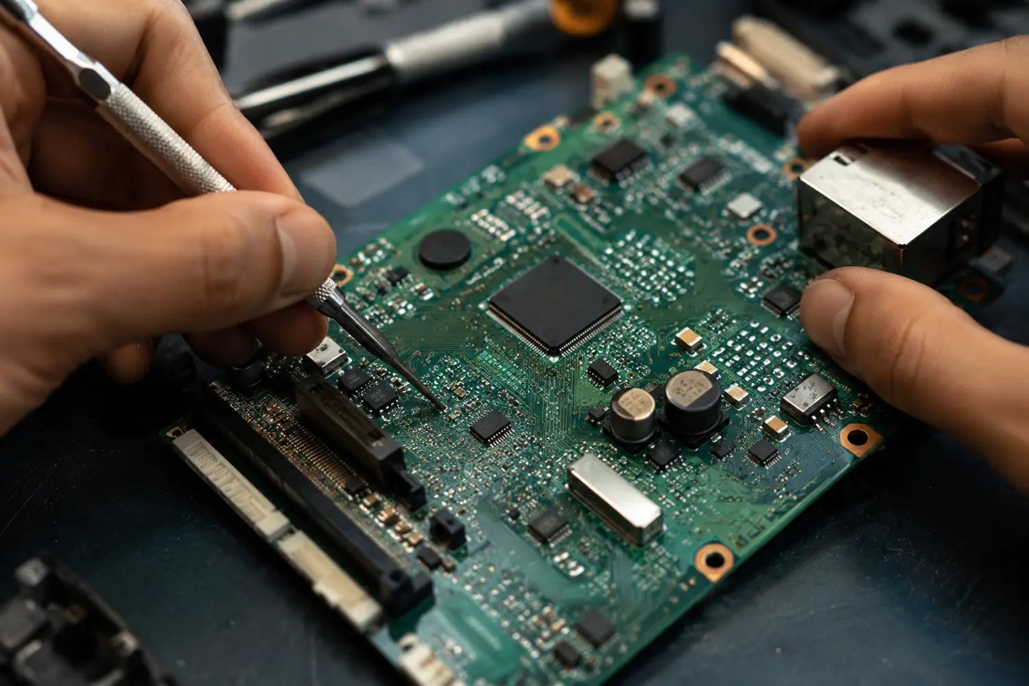
An electronic circuit board — formally known as a Printed Circuit Board (PCB) — is a flat, rigid (or sometimes flexible) board that mechanically supports and electrically connects electronic components using conductive pathways, or traces, etched from copper sheets laminated onto a non-conductive substrate.
Before PCBs, electronic devices were assembled using point-to-point wiring — a laborious, error-prone process where each component lead was manually soldered to terminal strips or tube sockets. The invention of the printed circuit board by Paul Eisler in 1936 (and its mass adoption by the U.S. military during World War II for proximity fuzes) revolutionized electronics manufacturing — enabling automated assembly, dramatic miniaturization, and vastly improved reliability.
Did You Know?
The term "printed" in printed circuit board refers to the original manufacturing process where conductive ink was literally printed onto an insulating board using a stencil — similar to silk-screen printing. Modern PCBs use photolithographic etching, but the name stuck.
2. The Anatomy of a PCB
Understanding a circuit board starts with understanding its layered construction. Every PCB, regardless of complexity, consists of several fundamental elements:
2.1 The Substrate (Base Material)
The substrate is the insulating foundation of the PCB. The most common substrate material is FR-4 — a flame-retardant woven fiberglass cloth impregnated with epoxy resin. FR-4 offers an excellent balance of mechanical strength, electrical insulation, thermal stability (Tg of 130-180°C), and cost. For high-frequency applications, specialized substrates like PTFE (Teflon), ceramic-filled hydrocarbon, or polyimide are used for their superior dielectric properties and lower signal loss.
2.2 Copper Foil
Thin copper foil — typically 0.5 oz/ft² (17 µm), 1 oz/ft² (35 µm), or 2 oz/ft² (70 µm) — is laminated to one or both sides of the substrate. This copper is etched away in specific patterns to create the conductive traces, pads, and planes that form the circuit. Heavy copper PCBs (4-10 oz) are used for high-current power applications.
2.3 Solder Mask
The solder mask is the thin, typically green (though available in red, blue, black, white, and yellow) polymer layer applied over the copper traces. It serves three critical functions: preventing solder bridges between closely spaced pads during assembly, protecting copper from oxidation and corrosion, and providing electrical insulation. The iconic green colour comes from the epoxy-based polymer used in the UV-curable solder mask ink.
2.4 Silkscreen
The white (or sometimes yellow) text and symbols you see on a PCB — component designators (R1, C3, U2), polarity markers, test points, company logos, and revision numbers — is the silkscreen layer. It's typically applied using an epoxy ink screen-printing process and serves as the human-readable reference for assembly, testing, and troubleshooting.
3. Types of Circuit Boards
PCBs come in several configurations, each suited to different complexity and cost requirements:
3.1 Single-Layer (Single-Sided) PCBs
The simplest type — copper on only one side of the substrate, components on the other. Used in low-cost, high-volume products like calculators, LED lighting, simple power supplies, and consumer toys. Single-layer boards are the cheapest to manufacture but offer limited routing density since traces cannot cross without using jumper wires.
3.2 Double-Layer (Double-Sided) PCBs
Copper on both sides of the substrate, connected by plated through-holes (vias). This doubles the available routing area and is the workhorse of general electronics — found in industrial controls, power supplies, instrumentation, automotive modules, and countless other applications. Double-layer boards allow traces to cross by transitioning between layers through vias.
3.3 Multi-Layer PCBs
Three or more copper layers (commonly 4, 6, 8, 12, up to 40+ layers for advanced designs) laminated together with insulating prepreg between each pair. Multi-layer boards enable extremely dense routing, dedicated power and ground planes, controlled impedance for high-speed signals, and superior EMI performance. They are used in smartphones, servers, networking equipment, aerospace avionics, and military systems.
3.4 Flexible & Rigid-Flex PCBs
Flex PCBs use a flexible polyimide (Kapton) substrate that can bend, fold, and conform to tight spaces — ideal for wearable devices, cameras, and applications where the board must fit into a curved enclosure or move during operation. Rigid-flex PCBs combine rigid FR-4 sections with flexible polyimide sections in a single board, eliminating connectors and improving reliability in applications like aerospace and medical implants.
4. Critical PCB Components Explained
A bare PCB is just a platform. It's the components soldered onto it that bring the circuit to life. Here are the essential component categories found on nearly every electronic circuit board:
4.1 Microcontrollers & Microprocessors
The "brain" of the board — a programmable integrated circuit that executes firmware instructions. Microcontrollers (MCUs) like the STM32, ESP32, ATmega328, and PIC families integrate CPU, RAM, flash memory, and peripherals (GPIO, ADC, timers, communication interfaces) on a single chip. Microprocessors (MPUs) are more powerful but require external RAM and storage — used in single-board computers like the Raspberry Pi and embedded Linux systems.
4.2 Voltage Regulators
Voltage regulators ensure that every component receives a stable, precise supply voltage regardless of input variations. Linear regulators (LDOs like AMS1117, LM7805) provide low-noise outputs for sensitive analog circuits. Switching regulators (buck, boost, buck-boost converters) achieve 85-95% efficiency for battery-powered and high-current applications.
4.3 Capacitors
Capacitors store and release electrical energy, performing multiple critical roles: decoupling/bypass capacitors (typically 100 nF ceramic) placed near every IC power pin to suppress noise; bulk capacitors (electrolytic, 10-1000 µF) for power supply smoothing; and tuning capacitors in RF and timing circuits. The right capacitor selection — considering capacitance, voltage rating, ESR, temperature coefficient, and package size — is fundamental to reliable design.
4.4 Resistors
The most numerous components on most boards — resistors limit current, divide voltages, set gain in amplifier circuits, pull signals to defined logic levels, and terminate transmission lines. Surface-mount chip resistors in 0402, 0603, 0805, or 1206 packages dominate modern designs, while through-hole resistors remain common in prototyping and high-power applications.
4.5 Connectors & Interfaces
The physical interface between the PCB and the outside world. USB (Type-A, Type-C, Micro-B), HDMI, Ethernet RJ45, board-to-board (pin headers, mezzanine), wire-to-board (JST, Molex, screw terminals), and RF connectors (SMA, U.FL) — each selected for its electrical, mechanical, and environmental specifications.
5. How PCBs Are Manufactured
The journey from a designer's CAD file to a finished circuit board is a fascinating multi-step process:
- Design & DFM Check: The PCB is designed in EDA software (Altium, KiCad, Eagle). A Design for Manufacturability (DFM) check verifies that trace widths, clearances, drill sizes, and annular rings meet the manufacturer's capabilities.
- Photolithography: The copper-clad laminate is coated with photoresist, exposed to UV light through a photomask of the circuit pattern, and developed — leaving resist only where copper should remain.
- Etching: The board is immersed in an etchant (typically ferric chloride or ammonium persulfate) that dissolves unprotected copper, leaving only the desired trace pattern.
- Drilling: CNC drilling machines create all through-holes and vias with carbide drill bits as small as 0.1 mm diameter. For HDI boards, laser drilling creates microvias.
- Plating: Electroless copper deposition followed by electrolytic copper plating metallizes the hole walls, creating electrical connections between layers.
- Solder Mask & Silkscreen: UV-curable solder mask ink is applied, exposed, and developed. The silkscreen legend is printed on top.
- Surface Finish: A protective finish (HASL, ENIG, OSP, immersion silver, immersion tin) is applied to exposed copper pads to prevent oxidation and ensure solderability.
- Electrical Test: Flying probe or bed-of-nails testing verifies that every net has correct continuity and no unintended shorts exist.
6. PCB Design Fundamentals
Good PCB design is both science and art. Key principles include: component placement that minimizes critical trace lengths and groups functional blocks logically; trace routing with controlled impedance for high-speed signals (typically 50Ω single-ended, 100Ω differential); ground plane integrity with no splits under critical signals; thermal management using copper pours and thermal vias; and EMI mitigation through proper stackup design, guard traces, and filtering.
7. Real-World Applications
Electronic circuit boards power virtually every technology sector. Smartphones pack 10-15 individual flex and rigid PCBs into a device just 7 mm thick. Modern vehicles contain over 100 PCBs controlling everything from engine timing to adaptive cruise control. Medical devices like MRI machines use massive multi-layer boards with ultra-low-noise analog front-ends. Satellite communication systems depend on space-qualified PCBs that survive extreme thermal cycling and radiation exposure.
8. Future Trends in PCB Technology
The PCB industry continues to evolve rapidly. Embedded components — resistors and capacitors fabricated inside the PCB substrate itself — save surface space and improve high-frequency performance. 3D-printed electronics are emerging for rapid prototyping and conformal applications. Optical PCBs with integrated waveguides for chip-to-chip photonic communication promise dramatic bandwidth improvements. And biodegradable substrates are being developed to address the growing e-waste crisis.
9. Conclusion
Electronic circuit boards are the unsung heroes of the digital age — invisible to most users but absolutely essential to every electronic device we depend on. Understanding PCB types, components, and manufacturing processes is the foundation of competence in electronics engineering, procurement, and product development.
At AEAR, we combine deep technical expertise with state-of-the-art manufacturing to deliver PCBs that meet the most demanding specifications — from simple double-sided prototypes to complex 20-layer HDI boards for mission-critical systems. Whether you need design support, prototyping, or volume production, our team is ready to partner with you.
AEAR PCB Capabilities at a Glance
✓ 1-24+ layer PCBs | ✓ FR-4, High-Tg, Polyimide, Rogers, Taconic substrates | ✓ HDI with laser-drilled microvias | ✓ Heavy copper up to 10 oz | ✓ Flex & Rigid-Flex | ✓ Surface finishes: ENIG, HASL, OSP, Immersion Silver/Tin | ✓ IPC Class 2 & Class 3 | ✓ Turnkey assembly available
Vikram Sharma
Really appreciated the step-by-step manufacturing process explanation. I'm new to PCB design and this article clarified so many concepts — especially the difference between solder mask and silkscreen. The FR-4 vs polyimide comparison was also very helpful.
Jennifer Tran
Embedded components are the future! We've started using buried capacitance layers in our high-speed designs and the improvement in PDN impedance is remarkable. Would love to see a follow-up article on that topic.
David Nguyen
Excellent overview. One correction: modern smartphones actually use mSAP (modified semi-additive process), not traditional subtractive etching, for their main boards — that's how they achieve sub-30μm trace/space. Still, great article for understanding the fundamentals.